Printing solar cells and organic LEDs

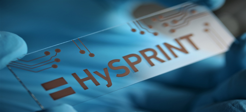
The HySPRINT logo (Helmholtz Innovation Lab) printed on a copper solution symbolizes how the thinnest material layers can be produced simply and cost-effectively. Possible applications are solar cells, organic LEDs or transistors. Photo © Humboldt-Universität zu Berlin/List-Kratochvil
Humboldt-Universität zu Berlin and Helmholtz-Zentrum Berlin form a joint lab and research group “Generative production processes for hybrid components”.
Solar cells, LEDs and detectors made of organic and hybrid semiconductors can nowadays be simply printed out, even together with teensy nanostructures that make them function better. The development of low-cost printing methods for electronic and optoelectronic components is at the centre of things for the new joint research group and the joint laboratory of the Helmholtz-Zentrum Berlin (HZB) and Humboldt-Universität zu Berlin (HU).
Cooperating together in the new research group are the HU workgroup “Hybrid Devices” led by Prof. Dr. Emil List-Kratochvil, the HZB young investigator group of Dr. Eva Unger, the Helmholtz Innovation Lab HySPRINT, and the Competence Centre Photovoltaics Berlin (PVcomB) directed by Prof. Dr. Rutger Schlatmann. The partners are building up a joint lab at Humboldt-Universität zu Berlin that will allow the researchers to acquire and use complementary laboratory infrastructures for various coating methods.
Prof. Emil List-Kratochvil is the head of the HU workgroup “Hybrid Devices” at IRIS Adlershof, and has been working for 15 years on developing electronic and optoelectronic hybrid components, resource-efficient deposition techniques (inkjet printing) and in-situ nanostructuring and synthetic methods. This expertise complements the aims of the HZB young investigator group led by Dr. Eva Unger. She will be developing solution-based manufacturing methods for depositing perovskite semiconductor layers onto larger surface areas for solar cells. “The new research group with List-Kratochvil is a real win for us. With his experience in printed electronic components, he is an ideal cooperation partner for us,” Unger says.
In recent months, the researcher and her team have already come much closer to her goal of developing hybrid tandem solar cells with large-surface-areas in the scope of the Helmholtz Innovation Lab HySPRINT. Now, the next step is to upscale the process in order to drive the novel solar cells towards market maturity. The Competence Centre Thin-Film- and Nanotechnology for Photovoltaics Berlin (PVcomB) is the ideal partner for the development of industrially relevant manufacturing processes. The joint research group is now striving towards building a pilot line on which to develop prototypes of hybrid components.
(sz)
https://www.helmholtz-berlin.de/pubbin/news_seite?nid=14922;sprache=en
- Copy link
-
Battery research with the HZB X-ray microscope
New cathode materials are being developed to further increase the capacity of lithium batteries. Multilayer lithium-rich transition metal oxides (LRTMOs) offer particularly high energy density. However, their capacity decreases with each charging cycle due to structural and chemical changes. Using X-ray methods at BESSY II, teams from several Chinese research institutions have now investigated these changes for the first time with highest precision: at the unique X-ray microscope, they were able to observe morphological and structural developments on the nanometre scale and also clarify chemical changes.
-
BESSY II: New procedure for better thermoplastics
Bio-based thermoplastics are produced from renewable organic materials and can be recycled after use. Their resilience can be improved by blending bio-based thermoplastics with other thermoplastics. However, the interface between the materials in these blends sometimes requires enhancement to achieve optimal properties. A team from the Eindhoven University of Technology in the Netherlands has now investigated at BESSY II how a new process enables thermoplastic blends with a high interfacial strength to be made from two base materials: Images taken at the new nano station of the IRIS beamline showed that nanocrystalline layers form during the process, which increase material performance.
-
Hydrogen: Breakthrough in alkaline membrane electrolysers
A team from the Technical University of Berlin, HZB, IMTEK (University of Freiburg) and Siemens Energy has developed a highly efficient alkaline membrane electrolyser that approaches the performance of established PEM electrolysers. What makes this achievement remarkable is the use of inexpensive nickel compounds for the anode catalyst, replacing costly and rare iridium. At BESSY II, the team was able to elucidate the catalytic processes in detail using operando measurements, and a theory team (USA, Singapore) provided a consistent molecular description. In Freiburg, prototype cells were built using a new coating process and tested in operation. The results have been published in the prestigious journal Nature Catalysis.
